

Semicon India Programme 2.0: Cabinet Approves Rs 1.27 Lakh Crore Chip Manufacturing Push
Semicon India Programme 2.0: Cabinet Approves Rs 1.27 Lakh Crore Chip Manufacturing Push
Relevance: GS Paper III (Science & Technology, Indian Economy, Infrastructure, Self-Reliance)
Why in the News?
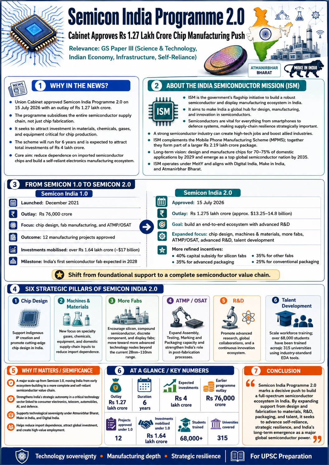
- The Union Cabinet approved the Semicon India Programme 2.0 on July 15, 2026, with an outlay of Rs 1.27 lakh crore.
- The programme focuses on subsidising the entire semiconductor supply chain — extending well beyond chip fabrication alone.
- It aims to attract investment in materials, chemicals, gases, and equipment critical for semiconductor production.
- The scheme runs for six years and is expected to attract total investments of Rs 4 lakh crore.
- Its core goal is to reduce India's reliance on imported semiconductor chips and build a self-reliant electronics manufacturing ecosystem.
About the India Semiconductor Mission (ISM)
- The ISM is a comprehensive government initiative to build a robust semiconductor and display manufacturing ecosystem in India, aiming to make it a global hub for design, manufacturing, and innovation in the sector.
- Semiconductors are foundational to modern electronics, from smartphones to defence systems, making supply chain resilience a strategic priority — especially given vulnerabilities exposed during recent global crises.
- A thriving semiconductor industry acts as an economic multiplier, creating high-tech jobs and boosting allied sectors.
- The mission complements the Mobile Phone Manufacturing Scheme (MPMS), together forming part of a larger Rs 2.19 lakh crore government package.
- The long-term vision: India aims to design and manufacture chips for 70-75% of domestic applications by 2029, and become a top global semiconductor nation by 2035.
- The ISM, operating under the Ministry of Electronics and Information Technology (MeitY), is the nodal agency implementing this programme.
- It aligns with broader national goals such as Digital India, Make in India, and Atmanirbhar Bharat.

From Semicon 1.0 to Semicon 2.0
- Semicon India 1.0 (launched December 2021, outlay of Rs 76,000 crore) laid the foundational groundwork and attracted initial investment, focusing on design, fab manufacturing, and ATMP/OSAT (Assembly, Testing, Marking, and Packaging/Outsourced Semiconductor Assembly and Test).
- Under 1.0, 12 manufacturing projects were approved, with cumulative investments exceeding Rs 1.64 lakh crore (~$17 billion), and the country's first semiconductor fab is scheduled for commissioning in 2028.
- Semicon India 2.0 (approved July 15, 2026, outlay of Rs 1.275 lakh crore, roughly $13.25-14.8 billion) builds on this momentum to create an end-to-end ecosystem with advanced R&D.
- It expands focus areas to: chip design, machines and materials, more fabs, ATMP/OSAT, advanced R&D, and talent development.
- Incentive structure under 2.0 is more refined: 40% capital expenditure subsidy for silicon fabs, 35% for other fabs, 35% for advanced packaging, and 25% for conventional packaging.
Six Strategic Pillars of Semicon India 2.0
|
1. Chip Design: Continued support for indigenous intellectual property (IP) creation and encouragement of cutting-edge chip design within India. 2. Machines and Materials: A new focus area subsidising critical supply-chain components — promoting domestic production of specialty gases, chemicals, and equipment, and aiming for self-sufficiency in key raw materials to reduce import dependence. 3. Setting Up More Fabs: Attracting capital for diverse fabrication units — including silicon, compound semiconductor, discrete component, and display fabs — and moving toward advanced technology nodes beyond the current 28nm-110nm range. 4. Strengthening the ATMP/OSAT Industry: Expanding Assembly, Testing, Marking, and Packaging facilities, and enhancing India's role in post-fabrication value chain processes. 5. Research & Development: Shifting focus toward more sophisticated R&D, fostering global collaborations with leading international R&D centres, and building a continuous innovation ecosystem. 6. Talent Development: Scaling up workforce training programmes to meet industry demands; over 68,000 students have already been trained across 315 universities using industry-standard Electronic Design Automation (EDA) tools. |
Significance
- Represents a major scale-up from Semicon 1.0, moving India from foundational investment attraction toward building a complete, self-reliant semiconductor value chain.
- Directly supports India's strategic autonomy in a critical technology sector with applications spanning consumer electronics, telecommunications, and defence.
- Reinforces India's broader technological sovereignty goals under Atmanirbhar Bharat, Make in India, and Digital India.